
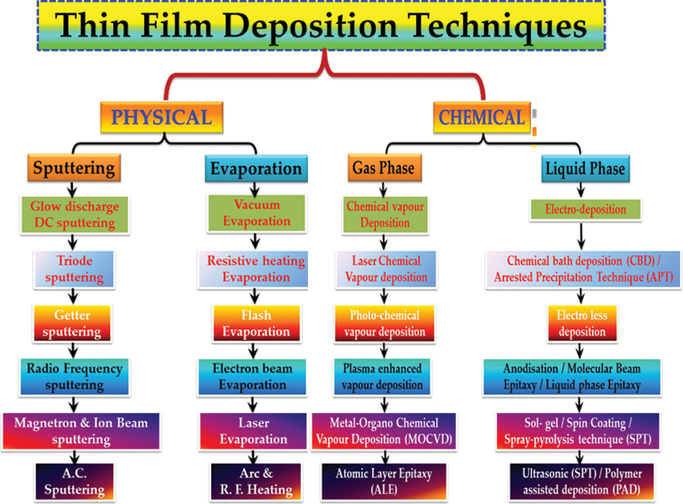
Know in detail about the thin film deposition its various types and applications
Thin Film Deposition
The action of applying a thin film to a surface is known as a thin-film deposition. Thin-film deposition is any procedure for depositing a thin film of material onto a substrate or onto formerly deposited layers. “Thin” is a relative word, but most deposition procedures allow layer thickness to be structured within a few tens of nanometers, and molecular beam epitaxy allows single layers of atoms to be deposited at a time.
It is useful in the production of optics (for reflective or anti-reflective coatings, for instance), packaging (Aluminium-coated PET film), electronics (layers of insulators, semiconductors, and conductors form integrated circuits), and in contemporary art. Similar processes are sometimes used where the thickness is not essential, for example, the deposition of silicon and supplemented uranium by a CVD-like process after gas-phase processing and the refinement of copper by electroplating.
Deposition procedures fall into two broad classes, depending on whether the process is primarily chemical or physical.
Chemical Deposition
Here, a fluid precursor undergoes a chemical transformation at a solid surface, leaving a solid layer. An everyday example is the development of soot on an object when it is placed inside a flare. Since the fluid surrounds the solid thing, deposition ensues on every exterior, with little regard to direction; thin films from chemical deposition procedures tend to be conformal, rather than directional.
Types of Chemical Deposition
Chemical solution deposition (CSD) aids a liquid precursor. Usually, a solution of organometallic powders liquified in an organic solvent. Plating depends on liquid precursors, often a solution of water with a salt of the metal to be deposited. Some plating processes are impelled entirely by reagents in the solution (usually for noble metals). However, by far, the most commercially important method is electroplating.
It was not generally used in semiconductor processing for many years but has seen a resurgence with the more widespread use of chemical-mechanical polishing procedures. This is a relatively economical, simple thin-film process that can produce stoichiometrically accurate crystalline phases.
Chemical vapour deposition (CVD) commonly employs a gas-phase precursor, habitually a hydride or halide of the element to be deposited. For instance, MOCVD, an organometallic gas, is utilised. Industrial procedures often use extremely low pressures of precursor gas.
Plasma enhanced CVD (PECVD) uses an ionised vapour, or plasma, as a precursor. Unlike the soot example above, commercial PECVD depends on electromagnetic potentials such as microwave excitation, electric current rather than a chemical reaction, to produce a plasma.
Physical Deposition
Physical deposition uses mechanical or thermodynamic means to produce a thin film of solid. An everyday instance is the formation of frost. Since most engineering resources are held together by relatively high energies, and chemical reactions are not used to store these energies. Commercial physical deposition methods tend to require a low-pressure vapour background to function properly; most can be categorised as physical vapour deposition (PVD).
The material to be deposited is engaged in an active, entropic environment so that particles of material escape its surface. Facing this source is a chiller that draws energy from these particles as they arrive, allowing them to form a solid layer. The whole method is kept in a vacuum deposition chamber, to allow the particles to travel as spontaneously as possible. Meanwhile, particles tend to follow a straight path, films deposited by physical means are commonly directional, rather than conformal.
Types of Physical Deposition
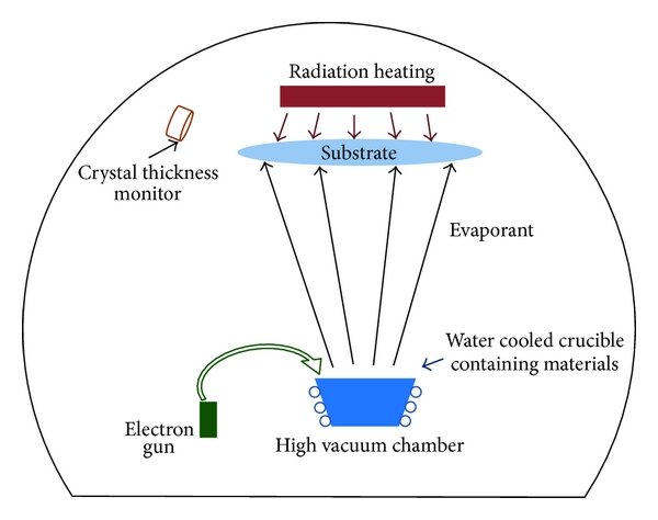
A thermal evaporator employs an electric resistance heater to melt the substance and raise its vapour pressure to a suitable range. This is done in an elevated vacuum, and both let the vapour to arrive at the substrate without changing with or scattering against other gas-phase atoms in the chamber and reduce the amalgamation of scums from the residual gas in the vacuum chamber.
Only materials with a much-elevated vapour pressure than the heating element can be deposited without the contagion of the film. Molecular beam epitaxy is a particularly high-level form of thermal evaporation.
An electron beam evaporator bonfires a high-energy beam from an electron beam gun to boil a small spot of matter; since the heating is not uniform, lower vapour pressure materials can be deposited. The beam is customarily bent through an angle of 270° in order to confirm that the gun filament is not openly exposed to the evaporant flux—typical deposition rates for electron beam vaporisation array from 1 to 10 nanometers per second.
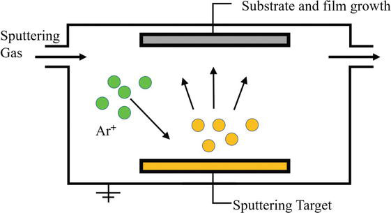
Sputtering relies on a plasma – usually a noble gas, such as argon to knock material from an ” aim at ” a few atoms at a period. A process used to deposit thin films of an object onto a substrate. By initiating a gaseous plasma and then quickening the ions from this plasma into some source material (target), the source material is eroded by the arriving ions via energy transfer. It is ejected in the form of neutral particles – either single atoms or clusters of molecules.
As these neutral particles are ejected, they will travel in a straight line unless they come into contact with other particles or a near-surface. The target kept at a comparatively low temperature. Subsequently, the process is not one of evaporation, assembling this as one of the most malleable deposition procedures. It is especially useful for compounds, where different constituents would otherwise tend to evaporate at different rates.
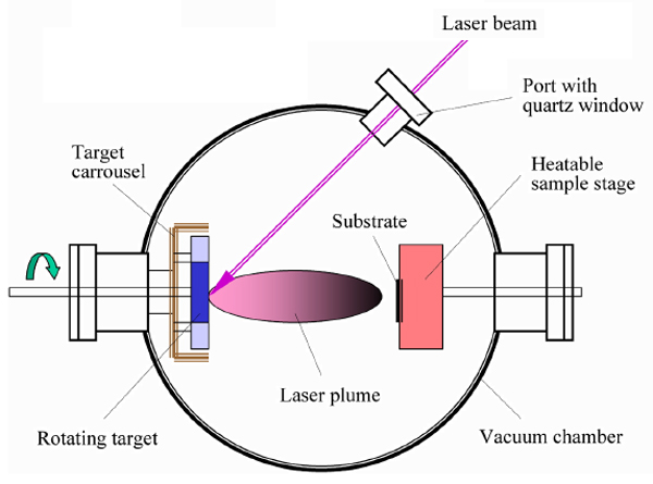
Pulsed laser deposition techniques work by an ablation process. Pulses of focused laser light turn vapour the surface of the target substance and convert it to plasma; this plasma usually regresses to a gas before it reaches the substrate.
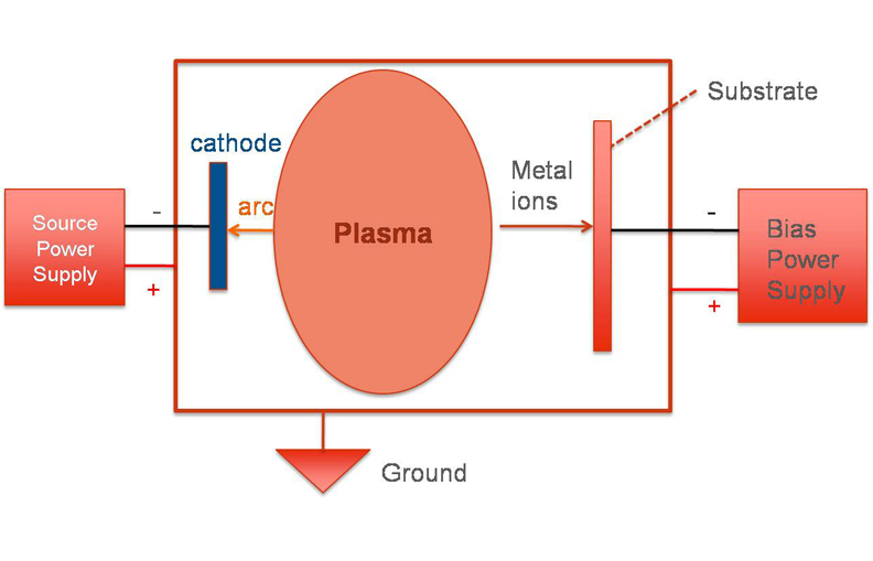
Cathodic arc deposition (arc-PVD) is a type of ion beam deposition where an electrical arc is created that blasts ions from the cathode. The arc has a remarkably high power density resulting in a high level of ionisation (30-100%), multiply charged ions, neutral particles, clusters, and droplets. If a reactive gas is commenced during the evaporation process, dissociation, ionisation, and excitation can occur during contact with the ion flux and a compound film will be deposited.
Now that you have read about Thin Film Deposition. Check out our course on Ampersand Academy Read this interesting article about Sol Gel Technique.